Has Etched begun shipping its AI inference hardware? The startup says it has delivered its first rack to Jane Street while raising $700 million at a $21 billion valuation. As inference workloads scale, memory bandwidth, interconnect latency, power delivery, and sustained compute utilization can become as important as peak arithmetic throughput. Traditional graphics processing units (GPUs) are designed to handle highly parallel workloads. However, autoregressive generation repeatedly moves model weights, KV-cache data, and intermediate state through the memory hierarchy, with access patterns varying by model architecture and serving configuration.
Why Etched’s First Rack Matters for AI Inference Economics
At a Glance
- Etched completed a $700 million funding round led by Jane Street, doubling its paper valuation to $21 billion within a single month.
- The company shipped its first inference rack to Jane Street, marking a key milestone as the quantitative trading giant begins to deploy the hardware in its workloads.
- Etched has secured over $1 billion in customer contracts across public and private AI companies, providing an early signal of customer demand.
The rapid growth of generative AI has increased demand for high-performance computing infrastructure. During the initial training era, standard graphics processing units were highly effective because model training relied on continuous backpropagation calculations. Training workloads can often expose more arithmetic parallelism than autoregressive decoding, making GPUs particularly well suited to large-scale matrix computation.
However, as applications transition to the inference era, the engineering requirements have changed. Unlike training, inference does not repeatedly update model weights; serving performance instead depends heavily on efficiently moving and processing model state under latency and throughput constraints. Depending on workload characteristics, memory bandwidth and interconnect latency can leave compute resources underutilized even when peak arithmetic throughput is high. Etched argues that sustained inference throughput on existing AI accelerators can remain well below peak FLOPs as thermal, memory, and interconnect constraints limit utilization.
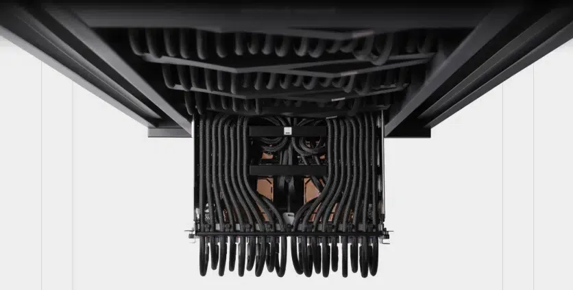
These constraints help explain why specialized inference hardware is attracting investment. Etched is pursuing a vertically co-designed inference system spanning silicon, racks, memory, interconnects, software, and manufacturing. Although the company was originally associated with a Transformer-specific silicon design, its current systems are designed to support a broader range of frontier model architectures, including mixture-of-experts (MoE) models and, according to company executives, non-Transformer architectures such as Mamba. By co-designing the entire execution stack, the custom hardware aims to reduce execution overhead. The trade-off is clear: the custom hardware is generally less flexible than general-purpose GPU platforms for workloads outside its targeted inference domain. Jane Street’s deployment provides an early signal of customer confidence in Etched’s architecture, although public data does not yet establish its production-scale performance or cost advantage over leading GPU systems, as discussed in TechCrunch’s reporting on the funding round.
Under-the-Hood Mechanics: Low Voltage Inference and Cluster Scale Memory
At rack scale, memory subsystems and scale-up interconnects can constrain how quickly model state moves between memory and compute resources. When an application executes an inference call, the processor must read data from memory, complete the operation, and write the output back. In standard configurations, these transfers can introduce latency and bandwidth pressure across the memory hierarchy and scale-up interconnect.
To address these inference bottlenecks, Etched combines two complementary architectural approaches for high-throughput and low-latency workloads:
Low Voltage Inference (LVI) and Cluster Scale Memory (CSM)
- Low Voltage Inference (LVI): Etched positions LVI primarily around high-throughput inference and describes it in the context of prefill-heavy workloads. Etched says lower-voltage math blocks allow substantially higher compute density within the available power and thermal envelope, while reducing exposure to power and thermal constraints.
- Cluster Scale Memory (CSM): CSM targets low-latency memory access and is designed to address the decode bottlenecks. Etched argues that today’s HBM-based AI systems struggle to achieve SRAM-level decode latency because of memory-subsystem and interconnect bottlenecks. CSM addresses this by connecting multiple chips via a proprietary high-bandwidth interconnect, creating a shared, low-latency memory pool across the scale-up domain.
A simplified mapping based on Etched’s description of prefill and decode workloads can be represented as:
[High-Throughput / Prefill-Heavy Workloads]
                     │
                     ▼
       [Low Voltage Inference — LVI]


[Low-Latency / Decode-Heavy Workloads]
                     │
                     ▼
       [Cluster Scale Memory — CSM]
By co-designing compute, memory, and interconnects, Etched aims to improve sustained inference utilization. Together, these approaches target different compute, memory, and interconnect constraints across inference workloads.
Specialized ASICs vs. General-Purpose GPUs: Evaluating the Specialization Trade-off
As modern computing environments move toward alternative hardware platforms, developers must re-evaluate how they manage execution stacks and computational workloads. The transition from general-purpose GPUs to application-specific integrated circuits (ASICs) represents a fundamental strategic choice. Engineering teams must weigh the potential efficiency advantages of dedicated hardware against the systemic risks of software lock-in and rigid architectural bounds.
Architectural Evaluation: Custom ASIC vs. General-Purpose GPU
Developing an ASIC requires substantial upfront engineering resources, long-term manufacturing agreements, and a stable, predictable workload profile. This approach can improve performance-per-token and cost efficiency when workload characteristics align closely with the hardware, but limits the platform’s ability to adapt if the underlying neural network architectures undergo a sudden paradigm shift. Conversely, GPUs benefit from a mature software ecosystem and generally offer greater flexibility when model architectures evolve, although workload-specific ASICs may offer stronger efficiency when the workload closely matches their architecture.
The table below outlines the core trade-offs between specialized ASICs and general-purpose GPUs:
| Dimension | Specialized ASIC | General-Purpose GPU |
|---|---|---|
| Workload Flexibility | Lower | Higher |
| Software Ecosystem | More specialized | Mature (e.g. CUDA) |
| Inference Optimization | Potentially high | Broad/general |
| Deployment Concentration Risk | Higher workload/vendor dependence | Broader ecosystem but still vendor-dependent |
| Scale Economics | Depends on workload fit and utilization | Established |
| Upgrade Flexibility | Lower | Higher |
Evaluating these hardware trade-offs is critical as organizations scale their active deployment clusters. While general-purpose GPUs remain the default for standard research and multi-model experimentation, specialized ASICs are increasingly appealing for high-volume, well-defined production workloads where minimizing latency is the primary operational objective.
Integration Checklists: How Engineering Teams Prepare for Hardware-Software Co-Design
To maintain execution stability and predictable performance as data centers adopt specialized inference hardware, engineering and product teams must adopt robust co-design workflows.
Developer Implementation Checklist
- Profile Model and KV-Cache Memory Requirements: Measure model weights, KV-cache growth, activation memory, and batch-size sensitivity under production traffic.
- Assess Model Architecture Compatibility: Verify that your production neural networks align with the hardware-level mathematical operators supported by the ASIC.
- Benchmark Core Execution Latency: Profile prefill and decode stages separately under realistic batch distributions to identify potential pipeline bottlenecks.
Product & Strategy Checklist
- Assess Workload Stability Before Hardware Specialization: Determine how frequently production model architectures change before committing to more specialized hardware.
- Audit Inference Economics: Benchmark throughput per dollar and per watt to justify the switching costs of adopting specialized hardware stacks.
- Verify System Scalability: Ensure that your hardware deployment plans account for raw material lead times and advanced packaging supply constraints.
By establishing these structured guidelines, development teams can transition their applications to more reliable and efficient inference deployments while maintaining operational continuity.
Frequently Asked Questions (FAQ)
When can a specialized inference ASIC outperform a general-purpose GPU?
How do Low Voltage Inference and Cluster Scale Memory resolve prefill and decode bottlenecks?
What is the biggest business risk of adopting specialized inference hardware?
Key Takeaways for Engineering Teams
Etched’s first rack shipment gives the company something its $21 billion valuation previously lacked: a real customer deployment. Jane Street’s early adoption and more than $1 billion in reported contracts strengthen the demand case, but contracts and early testing are not the same as proven large-scale economics.
The technical bet is broader than a single chip. Etched is co-designing silicon, memory, interconnects, racks, and software around inference workloads, using LVI for high-throughput operation and CSM for low-latency memory access. For buyers, the central question is whether those efficiency gains can outweigh the flexibility, ecosystem maturity, supply-chain resilience, and upgrade path offered by general-purpose GPUs.
References
-
Etched. From Zero to One: Shipped First Customer Delivery. https://www.etched.com/progress/from-zero-to-one
-
Reuters. AI chip startup Etched valued at $21 billion in latest funding round. https://www.reuters.com/technology/ai-chip-startup-etched-valued-21-billion-latest-funding-round-2026-08-18/
-
TechCrunch. Etched’s valuation doubles to $21B in a month. https://techcrunch.com/2026/08/18/etcheds-valuation-doubles-to-21b-in-a-month/
-
TechCrunch. AI chip startup Etched defies skeptics, hits $10.3B valuation from big-name investors. https://techcrunch.com/2026/07/23/ai-chip-startup-etched-defies-skeptics-hits-10-3b-valuation-from-big-name-investors/
Share this article