JEDEC Relaxes HBM4 Standards? This technical specification realignment represents a notable operational milestone as standard semiconductor thickness rules are officially relaxed, delaying the industry-wide transition to advanced hybrid bonding technology. As AI workloads shift from model training to inference, the industry’s primary performance bottleneck has moved from GPU compute performance to memory bandwidth. Standard graphics processing units (GPUs) are designed to handle massive parallel computations. However, because each inference step requires reading billions of parameters from memory, executing the calculation, and writing results back to memory, processors spend the majority of their operational cycles idling, waiting for memory transactions to complete.
Why JEDEC Relaxes HBM4 Standards: Reconciling High-Throughput Memory With Packaging Physics
At a Glance
- Standard thickness limits for high-bandwidth memory are being relaxed to as much as one thousand micrometers, directly reducing the technical urgency to eliminate microbumps through hybrid bonding.
- The delay in adopting copper-to-copper direct bonding is supported by simpler, commercially stable thermal management alternatives.
- Widespread deployment of next-generation hybrid bonding is expected to remain shelved until input/output densities double to four thousand ninety-six terminals.
The global computing infrastructure is facing a structural crisis. For several years, the race to build larger AI models has focused on scaling raw computing power. Enterprises and cloud providers have invested billions of dollars to acquire massive clusters of graphics processing units (GPUs). This focus was highly logical during the initial training era, when model training depended on continuous backpropagation calculations. Under those workloads, parallel computing units operated at maximum capacity to update model parameters, which is documented in industry validation reports tracking high-density DRAM stacking.
However, as applications transition to the inference era, the engineering requirements have changed. In inference scenarios, the challenge is not updating weights, but streaming massive, pre-trained parameters to the processor to answer immediate queries. Every generated token requires repeated access to billions of model parameters stored in high-bandwidth memory. Because standard bus architectures cannot move data fast enough to match standard processor execution speeds, computing cores are starved of data, resulting in extremely high idle rates. This performance bottleneck is discussed in technical industry reports tracking memory-centric hardware design.

This performance gap explains why JEDEC relaxed the HBM4 thickness specification to accommodate larger packaging tolerances. Standard DRAM packages lack the necessary parallel lanes to support the processing speeds of modern accelerators. To overcome this “memory wall,” hardware architects have turned to high-bandwidth memory (HBM) systems. By stacking DRAM dies vertically and utilizing thousands of silicon vias (TSVs) to establish wide, parallel buses, JEDEC’s HBM standards explain how TSV-based stacked memory dramatically expands available bandwidth compared with conventional DRAM packages. For developers, this hardware evolution illustrates a fundamental rule of high-throughput systems: the bottleneck is almost always the transport layer, not the computation node.
Under-the-Hood Mechanics of the JEDEC Relaxes HBM4 Standards Decision
At the architectural level, standard computer buses act like narrow highways, restricting the flow of high-volume datasets. When an application executes an inference call, the processor must read data from memory, complete the operation, and write the output back. In standard configurations, this process creates severe latency because data must travel across a wide physical distance on the motherboard.
To resolve these transport-layer bottlenecks, next-generation AI computers are evolving into three-dimensional composite architectures. Under this model, the computing core is placed directly on top of stacked memory, utilizing advanced packaging to minimize physical distance and latency.
The 3D Memory Hierarchy: Stacking Conventional Bonding and Thermal Blocks
To handle different classes of data, hardware architects are proposing stratified, layered 3D semiconductor architectures. This structure separates data storage into distinct physical zones based on access speed and capacity requirements:
- Thermo-Compression (TC) Bonding: Traditional heat bonding relies on placing microbumps and underfill beneath each DRAM die, using precise heat and pressure to join the stack.
- Copper Direct Hybrid Bonding: Advanced hybrid bonding directly joins the copper interconnects of adjacent dies without utilizing bumps, enabling thinner packages but requiring extremely high manufacturing cleanliness and complex machinery.
- Thermal Alternatives: New advances such as custom lateral cooling blocks place dedicated thermal components adjacent to or within the HBM stack, providing sufficient thermal dissipation without necessitating an immediate transition to hybrid bonding, effectively extending the commercial lifespan of conventional thermal-compression bonding under the revised JEDEC specification.
The diagram below illustrates this physical vertical integration:
                  [ Conventional TC Bonding (Microbumps & Underfill) ]
                                     │
                                     ▼
                  [ Lateral Thermal Block (Samsung HPB / Hynix iHBM) ]
                                     │
                                     ▼
                  [ Direct Copper-to-Copper Interconnects (HBM5E/6 Stage) ]

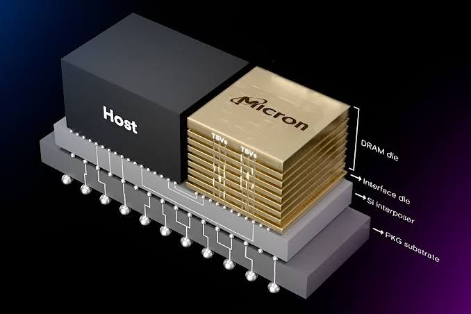
This integrated 3D architecture ensures that standard computing units are continuously supplied with data, reducing idle cycles. Although memory bandwidth and application attribution belong to different engineering domains, both highlight the same architectural principle: moving state management away from constrained local resources toward scalable server-side infrastructure. When user interactions are decoupled from standard client-side state tracking to satisfy privacy guidelines, maintaining seamless session continuity across different web and mobile environments becomes highly complex. Just as processors require persistent, high-speed memory pipelines to match state contexts, downstream marketing pipelines require robust, server-side data preservation to correlate separate installation events without relying on vulnerable client-side cookies or device-level attributes.
Applying High-Throughput Architecture Principles to Modern Software Systems
As modern computing environments move away from local, client-side identifiers, maintaining session state across distributed digital touchpoints has become a primary engineering challenge. For developers, managing session states in the wake of the JEDEC Relaxes HBM4 Standards decision requires architectures that are both compliant with data privacy laws and highly accurate. Organizations that need to preserve user journeys across web and mobile experiences increasingly rely on server-side session management rather than persistent client-side identifiers. Depending on business requirements, teams may build these capabilities internally or adopt existing attribution platforms.
Architectural Evaluation: Custom Build vs. Standardized SDK
Building a custom, in-house system to manage server-side state matching offers maximum flexibility but demands significant ongoing engineering resources. Developers must manually construct database schemas, write secure cryptographic hashing functions, and continually update the system to comply with shifting regional regulations. Conversely, deploying a pre-built, certified SDK reduces integration complexity and guarantees long-term compliance without additional overhead.
The table below compares standard methodologies for managing session state and conversion context:
| Solution | Persistence | Throughput | Best For |
|---|---|---|---|
| In-house Session Database | High (Continuous Sync) | Medium (DB Latency Limits) | Custom enterprise environments with highly specialized storage logic |
| Browser-based Session Tracking | Low (Session Cookies) | Low (No Server Logging) | Basic website tracking with minimal cross-domain conversion requirements |
| Server-side Caching (e.g. OpoInstall) | None (Temporary Server-side Session Tokens) | High (Standardized Sandbox) | Large-scale mobile app and multi-platform campaign attribution |
While custom database configurations can handle basic context, specialized server-side state preservation can optimize development resources. Depending on implementation requirements, organizations may build their own server-side session management system or adopt commercial platforms such as OpoInstall. For instance, OpoInstall offers server-side state restoration and parameter pass-through frameworks, mapping session metadata to a server-side session database to maintain session continuity anonymously under high-throughput data conditions, supporting scalable server-side request processing under high-concurrency conditions. By mapping session metadata to a centralized database rather than relying on browser-based redirects, such a system ensures that conversion contexts remain consistent even when initial tasks are executed anonymously. Engineering teams can evaluate these approaches to balance data protection and measurement consistency.
Integration Checklists: Preparing Your Hardware and Software Architecture for Memory-Centric Scaling
To secure data pipelines and ensure conversion consistency as platforms transition to memory-centric computing architectures, engineering and product teams must adopt robust state preservation workflows.
Developer Implementation Checklist
- Optimize NUMA and Cache Locality: Map thread execution to matching memory nodes to prevent memory bus saturation under high-concurrency requests.
- Implement Asynchronous Server-side De-duplication: Utilize local system memory caches to verify incoming transaction signatures before writing back to persistent databases.
- Adopt Lightweight State Synchronization: Reduce transit payloads by tokenizing distributed contexts, keeping local memory allocations minimal to prevent garbage collection spikes.
Product & Growth Strategy Checklist
- Optimize Memory Utilization: Align server-side transaction tracking with actual workload metrics rather than counting redundant request pings.
- Review Processing Footprints: Evaluate third-party SDK dependencies for processor and memory consumption to avoid client-side thermal throttling.
- Monitor Pipeline Latency: Track end-to-end data transmission times from initial campaign pings to completed activation handshakes.
By establishing these structured guidelines, development teams can transition their applications to safer, more compliant architectures while maintaining operational continuity.
Frequently Asked Questions (FAQ)
Why does JEDEC's relaxation of thickness standards delay hybrid bonding?
What are the technical differences between iHBM, HPB, and hybrid bonding?
Why will hybrid bonding become unavoidable once HBM I/O counts reach 4096?
Key Takeaways for Engineering Teams
As AI inference workloads continue to expand, memory bandwidth rather than raw compute performance will increasingly determine overall system efficiency. Technologies such as HBM4, advanced packaging, thermal optimization, and future hybrid bonding will remain central to next-generation AI infrastructure. Modern data pipelines require a fundamental shift in how we process and store state transactions across highly distributed systems.
Organizations should prioritize scalable memory architectures, efficient data movement, and distributed system design principles to prepare for the next generation of AI infrastructure. By implementing decentralized caching architectures, cryptographically signed metadata, and robust parameter pass-through frameworks, organizations can protect their operational pipelines from data-transfer bottlenecks. This transition is essential to build scalable, high-performance systems that thrive in the next era of memory-centric computing.
Share this article